
Turns out — computers aren’t getting faster anymore. So much for progress in the world of bits. For decades, the world has been transformed by the reality of Moore’s law, the expectation that the chips powering our computers would double in computational power every two years while falling in energy usage and price.
This phenomenon is responsible for creating the most valuable companies on Earth while completely redefining humanity's relationship with technology, which is why it’s particularly startling that all that is now in the past.
“Moore’s Law is dead,” pronounced Nvidia’s CEO, Jensen Huang in September, before adding “the idea that the chip is going to go down in price is a story of the past.”
Today’s chips come packed with billions of transistors, capable of executing billions of instructions per second. The smallest transistors on the market are now hitting the 3-nanometer mark, a length equivalent to 15 Silicon atoms. Though as going ever smaller presents tremendous financial, let alone physical challenges, many are bracing themselves for a world where achieving our digital dreams is only going to get more expensive from here.
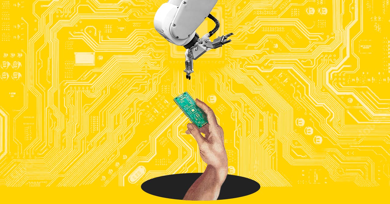
Currently, every major company that relies on computing is exploring ways to approach this new normal. Some are rethinking the designs of chips in their devices while others are beefing up the number of silicon experts they have in-house. The following piece traces the evolution of chip economics and design to better understand how we got here, and explore what the future might look like as a new chapter opens up in the world of hardware.
The Flow of Electricity
Electricity plays a crucial role in computers. It represents the physical form of information. So, to manipulate information, we first needed to figure out how to manipulate the flow of electricity.
In the early twentieth century, one of the biggest puzzles in electrical engineering was finding a mechanism that could switch electrical signals on and off — using electrical signals themselves. In 1911, Palo Alto native Lee DeForest figured out one of the first ways of doing it when he discovered the vacuum tube.
A vacuum tube is a glass vial with two components. A cathode at one end, which heats up and produces a stream of electrons, and an anode at the other end. By regulating whether or not a voltage is applied to the anode, you can control whether electrons will be permitted to pass across the vacuum from the cathode end to the anode end, powering a circuit.
These circuits, made by soldering together vacuum tubes, copper wires, and other rudimentary electrical components, could be assembled to perform basic logic functions. If you put enough logic functions together, you could make a primitive calculator — one that could do basic addition, subtraction, division, and multiplication. The University of Pennsylvania's ENIAC, built in 1946, was one of the first attempts at a large-scale electrical computer that could perform these calculations. But, it was composed of 18,000 vacuum tubes, miles of copper wire, and required 150,000 watts of power to operate. There was a rumor going around that whenever the ENIAC was switched on, the lights in Philadelphia dimmed.
The vacuum tubes would glow with heat, which required fans to cool them down. The glowing also attracted moths, which would short-circuit the machine, requiring engineers to literally de-bug it.
An improvement on glowing-hot vacuum tubes soon arrived from Bell Labs, where researchers were experimenting with a new class of materials they called semiconductors. Somewhere in between a conductor, like a metal, and an insulator, like glass, semiconductor materials selectively allow electrical current to flow through them. The trick was to figure out how to make the semiconductors allow current to flow through them when prompted.
The breakthrough came in 1947 from John Bardeen and Walter Brattain, a duo working under the guidance of William Shockley at Bell Labs. Together, Bardeen and Brattain built the first working prototype of a solid-state electrical switch, the transistor. Transistors allowed electricity to flow selectively through solid material, rather than having to detour through fragile and hot glass bulbs. That meant smaller circuits that could be turned on and off faster and use less energy.
Two years later in an interview, Shockley said, "There has been a great deal of thought spent on electronic brains, or computing machines. It seems to me that in these robotic brains, the transistor is the ideal nerve cell."
![]()
The Integrated Circuit
Shockley realized the transistor would soon take over the world of electronics, replacing everything that was touched by vacuum tubes. He started his own company, 'Shockley Semiconductors' to start mass manufacturing the devices, and sought out America's finest minds to help him. That quest led him to Robert Noyce, a physicist from MIT, and Gordon Moore, a chemist from Caltech. Shockley certainly had the right idea, but he was a deeply unpleasant personality. Within a year of signing up to work with him, all the engineers Shockley hired walked out to start their own company instead.
That operation, named Fairchild Semiconductors, after their main backer, was arguably Silicon Valley's first 'startup'.The opportunity of mass-producing transistors was unparalleled, but the experience of making them was hell. The transistors were tiny, and still needed to be hand-soldered to other electrical components, which was a grueling, inaccurate, and frustrating feat of human labor.
Rather than spend hours hunched over a soldering iron, Robert Noyce figured it might be a better idea to etch the complete circuit, transistors, wires and all, onto one solid wafer of semiconductor material. The integrated circuit was born. "I was lazy," said Noyce, reflecting on his bout of genius, "it just didn't make sense having people soldering together these individual components."

The etching was done by a process called photolithography, which shone light rays at silicon treated with light-sensitive material that hardened when exposed to light. This process allowed manufacturers to produce the circuit's grooves. Year after year, photolithographic techniques got better and better, which allowed Fairchild to make their circuits more and more complex.
The first integrated circuit made by Fairchild Semiconductors had only a single transistor, capable of completing just one logic function. By 1968, the transistors on Fairchild's integrated circuits numbered over a thousand.
As integrated circuits got smaller, they started to be called chips, but despite the cutesy name, something remarkable was happening on the surface of these chips. The smaller the transistors got, the smaller the current needed to activate them, and the smaller the transistors, the more transistors you could fit on the same chip. In perhaps the greatest example of economies of scale in history, the tinier transistors got, the more computation you could do for less power. The economics of miniaturization were so good they were almost unbelievable. By scaling down the size of a transistor by two, you scaled up the computational power by a factor of eight!
Naturally, this begged the question of how far this miniaturization could go. Already by 1965, Gordon Moore had predicted, or maybe prophesied, that the number of components on a chip would double every two years. But Moore's colleague at Caltech, the engineer and physicist Carver Mead wanted an answer to how small these transistors could get. After all, transistors were just little gates that allowed electrons to flow through when activated and blocked electrons when deactivated. The gates, in theory, could get really small indeed. Though the technology didn't exist to make transistors this small yet, Mead theorized that you could theoretically get them small enough to fit something like 10^7 to 10^8 onto an area of 1cm^2.
For 1971, these claims were outrageous. At the time, integrated circuits only had about 1000 transistors on them, but Mead was predicting an improvement of 5 to 6 magnitudes. While many academics and computer specialists were busy doubting Mead's predictions, Gordon Moore was already working tirelessly to make them a reality.
The Central Processing Unit
By 1968, Fairchild Semiconductor was a big, clunky company with 30,000 employees. It wasn't a startup anymore — it was, as Robert Noyce put it, a supertanker. In order to compete with the fast-moving world of electronics, Noyce and Moore left Fairchild to start a new, nimbler venture. They called their new company Integrated Electronics, which they shortened to Intel.
Right around the seventies, these integrated circuits were starting to count pretty well, but they couldn't remember much. Noyce and Moore figured that if transistors could increase the speed and energy efficiency of processing logic functions, maybe they could do the same for memory storage.
Intel's first product was the 1103 — a semiconductor-based memory chip. Transistors would open and close to either store or release an electric charge, thereby storing or releasing information.
The insight for Intel's next great invention came from Ted Hoff, an engineer who wondered what might happen if you could integrate both a 1103 memory chip and a processing unit all into the same integrated circuit. The result was the 4004 chip, released in the third year of Intel's existence. The 4004 wasn't just a chip, it was an entire computer on a chip! It cost $360, had 2,300 transistors, could perform 60,000 instructions per second, but most importantly, it could execute instructions stored in a memory bank and had working "scratch pad" memory to help it complete more complicated calculations.
This made it the first generally programmable 'central processing unit' or CPU, and it was a game changer. Ted Hoff later said, "With this product, we changed people's perception of computers and the direction that the computing industry would go. We democratized the computer."
The year after Intel released the 4004, they released the 8008, then in two years the 8080, which was ten times faster than the 4004, but still cost the same $360.
The fact that a generally programmable computer could be not only affordable, but also the size of a thumbnail, gave rise to the idea that computers weren’t just for offices anymore. Soon, each person could have a computer of their own.
The Altair 8800, released in 1975, was the first attempt at a 'personal computer.' It was powered by the Intel 8080 chip, had only 250 bytes of memory, and could be programmed by flipping a bunch of mechanical switches. Remarkably, 25,000 Altairs 8800s were sold for $1,000, just enough for the producers to break even. The Altair may not have had much staying power, but in the wake of its rollout, things moved fast.
Later that year, Bill Gates and Paul Allen launched Microsoft, whose first product was an interpreter that helped users program their Altair 8800s. Two years later, in 1977, Steve Wozniak and Steve Jobs released the Apple II, a personal computer decked out with a monitor and the first commercially available graphical user interface, and powered by the MOS 6502 CPU, a chip rivaling Intel's.
Intel's invention of a CPU that programmers could write their own code for gave birth to the personal computing movement. However, it was only when IBM, the largest computer company in the world, started ordering CPUs from Intel to produce its line of PCs that Intel's dominance over the computing industry was set.
General Purpose Chips
IBM flooded Intel with orders. To meet the demand, Intel had to start licensing its chip designs, called instruction set architectures, to other semiconductor foundries.
The instruction set architecture provides a complete description of a chip. It defines which instructions the processor can perform, what data types it can read, how memory is managed, along with a host of other things.
All of Intel's chips were being built to the specifications of their x86 architecture, and given the massive demand for Intel chips, soon nearly all semiconductor foundries were manufacturing chips according to Intel's x86 model too.
Manufacturing chips according to one set of specifications made it easier on semiconductor foundries and on software writers, who could be sure that their programs would be compatible with any chip as long as it was designed to x86 standards. But the extreme standardization was bad news for any other companies hoping that their chip designs would see the light of day.
The world of personal computing simply wasn't big enough for multiple versions of CPU architectures, and the fact that Intel's x86 model won out meant that many competing integrated device manufacturers fell by their wayside.
Given the landscape, most companies working on chips had to pick if they wanted to focus on designing and selling their own chip designs, and risk never getting any customers, or focus on fabricating someone else's designs, an increasingly competitive field where costs of production were starting to rise.
By 2000, regularly available CPUs had nearly 10 million transistors. The transistor gate lengths were becoming smaller than the wavelengths of light and therefore invisible to the human eye. Manufacturing integrated circuits at such a tiny scale was becoming a more expensive operation, to the point that soon, foundries were starting to out-innovate Intel. In 1999, TSMC, Taiwan Semiconductor Manufacturing Company, was the first semiconductor foundry to make transistors that were 180 nanometers wide.
Year after year, the cost of producing smaller transistors pushed more and more foundries out of business. Getting your hands on the increasingly esoteric photolithography instruments required deep pockets, and not everyone could cough up the cash. In the following years, the semiconductor industry saw wave after wave of corporate consolidation and mergers.
As the struggle to miniaturize grew and progress slowed, the first predictions of an end to Moore's Law started rolling in — often from Gordon Moore himself. Many just couldn't see how it would be economical to continue making transistors smaller.

To ensure continued improvements for consumers, CPUs started being designed with multiple processor cores. Rather than having one CPU in your computer, why not have two or three, which can handle twice or three times as many instructions at the same time? It soon became standard for most machines to start processing in 'parallel'. Right now, your computer is doing many tasks at once, it's retrieving information from the Internet, connecting with Bluetooth devices, refreshing your screen, alongside running many other programs. It's doing all of that and more through the help of parallel processing.
Parallel processing helped computers execute lots of independent tasks at the same time, and even the mere ability to do this ushered in a new era of computational possibility.
For one thing, parallel processors made it possible for the Internet to be used by billions around the world at the same time. Servers in data centers are packed with dozens of processor cores, each of which is busy connecting dozens of clients to web pages.
For another, complicated matrix multiplication, a key feature of neural network calculations, was perfectly suited for parallel computation. Feeding big neural network problems into powerful multi-core processors was a watershed moment in producing more powerful AI algorithms, and marked a renewed interest in artificial intelligence, which once again seemed feasible after the field suffered years without any progress.
Special Purpose Chips
The hidden secret of the digital revolution lay in the consistently improving computational ability made possible by making transistors smaller, and putting more of them into our computers. Today, the smallest transistors we manufacture are somewhere around 3nm wide, but it's a challenge. 3nm is roughly the width of 15 Silicon atoms end-to-end, and at the atomic scale, weird stuff happens. With transistors this small, electrons don't always behave as assumed. Rather than flowing through the circuit as expected, at this scale electrons sometimes jump across into neighboring circuits, a phenomenon called electron tunneling, which totally messes up the function of the computer.
![]()
Semiconductor companies have devised lots of mitigating strategies to address these defects but incorporating them into integrated circuits only makes producing chips more expensive. Furthermore, given the number of defects in manufacturing chips has increased, the yield of functional chips from running fabs at this scale has declined. In 2015, the cost of producing each individual transistor started increasing, a remarkable reversal in the economics of Moore's Law.
Ever since writing his 1971 paper anticipating that chips would see 10^8 transistors over 1cm^2, Carver Mead's then outrageous predictions have proved conservative in an era that can see over 6x10^9 over the same area. However, like any great physicist, Mead knew that no exponential lasts forever.
He too, had been anticipating the end of Moore's Law for quite some time and had criticized the industry's tunnel vision over transistor density when the real improvements in computational speed might be found elsewhere entirely.
“The semiconductor guys don’t know much about computers so they’ve copied a bunch of ancient architectures. So what we have in the personal computers is creaky old architectures with this wonderful [semiconductor] technology. So the people driving the technology don’t know anything about systems and the people who have built traditional large computer systems haven’t participated in the [semiconductor] technology revolution," he said.
At the end of the day, the speed of computation is determined by how quickly electrons can move from point A to point B to complete their instructions. The idea that all computations should be run through the same, standardized, general-purpose hardware architecture to complete those instructions is a huge bottleneck in computational efficiency.
If you want to compute something really fast, you probably don't have time for the software you write to be compiled into x86 machine code and then executed. Instead, Carver Mead suggests that you map your program directly into the silicon. "The technology for doing that we understand pretty well. We’ve developed the technology for taking high-level descriptions and putting them on silicon. It’s called silicon compilation, which is the obvious next step. You need to compile things right down into the chip instead of compiling them into some code that you feed to this giant mass of chips that grinds away on it trying to interpret it,” said Mead.
The concept of producing application-specific integrated circuits is exactly what transpired. They're called ASICs for short. The most popularly recognizable variety of ASIC is probably the Bitcoin miner. These are processor chips whose circuits are designed specifically so they can be hyper-efficient at running the SHA-256 algorithm, and thereby mine Bitcoin.
However, the idea of making application-specific chips doesn't just end with Bitcoin. Virtually every company that produces a device that relies on an integrated circuit has realized that sooner or later, they're going to need to start producing chips customized to their applications. The old Intel model of buying an off-the-shelf chip and sticking it into your product just isn't going to cut it anymore, especially in an era where you can't count on Moore's Law to deliver future improvements in performance.
All chip design shops from Intel to Nvidia to Qualcomm are now facing the existential question of what to do when modern technology companies start hiring their own chip engineers capable of designing specialized integrated circuits.
In 2020, Apple moved away from using Intel chips to power its MacBooks after designing a specialized M1 chip, based on a different and faster kind of CPU architecture, called ARM, most commonly seen in smartphones. The real innovation of the M1 chip was to design a smarter placement of memory and processor centers so that information could flow faster between the two, thereby executing instructions faster. The decision to start making their own chip designs was a terrifically successful move for Apple, as their M1 chip is now considered the fastest CPU on the market.
The world of data centers has also seen a proliferation of specialized chip models. Amazon and Microsoft, running massive proprietary data centers, both now have teams that design chips tailor-made for their respective servers.
And in the realm of AI, Google revealed the design of its Tensor Processing Unit in 2016, a chip specifically designed to run Google's TensorFlow AI algorithm. Similarly, in 2022, Tesla announced that it has developed its own specialized Dojo chip too!
A Wild West of Hardware
Hitting the physical limits on transistor length is an exciting, if uncertain moment in the computing industry. It means that new techniques will need to be pursued to gain improvements in computing speeds, and it also means the way we think about computing might start to move away from a framework that to date, has been dominated by the constraints of standardized chip architectures.
Designing microelectronics will have to become synonymous with computer science, and the gap in understanding between hardware and software will need to close. As the great computer scientist Alan Kay once said, "people who are really serious about software should make their own hardware."
And whereas the path to 'making your own hardware' used to seem nearly impossible, it might actually be closer than we think. One of the biggest barriers to designing chips is the fact that making custom chips takes a long time — often years. Many of the design steps still require lots of manual review, however, the timeline might soon shrink as new solutions are emerging that can make the process more efficient. Google is working on producing a machine learning model that can assist chip designers in "chip floorplanning," a crucial step involved in designing chips. Earlier in 2022, Google also revealed a program that lets chip designers access open-source software for chip designing, even allowing users to print designs for free with partner fabs.
In due time, researchers and entrepreneurs like Anders Olofsson are anticipating we might see faster growth in the open-source hardware community, as Carver Mead's vision for "silicon algorithms" and more widespread use of silicon compilers becomes more of a reality.
There are even some doing research at the level of fundamental physics to find new, tinier materials which could succeed at making circuits faster and smaller. One such effort involves replacing silicon channels with circuits made of carbon nanotubes. Another is interested in replacing the electrons in those channels with tinier and faster-moving photons.
Until such breakthroughs succeed in producing commercially feasible products, many of us will have to reckon with a new digital normal. A world without ever-smaller circuitry will certainly need a new computational paradigm, one that moves away from a chip-for-all framework, and toward a world of new and more varied chip architectures and devices. The computer scientists of the future will need to understand not only the software but also the hardware on which their algorithms run, presaging a time when physics will rear its head yet again in our study of digital devices.
Below are the companies working on the biggest challenges in chip production and design:
- ZeroASIC is working on creating more powerful architectures for parallel processors while working on democratizing access to silicon technologies.
- Volantis Semi is creating fault-tolerant chip architectures that would improve the yields on 3nm and smaller fab processes, betting that the computational gains from further miniaturization will outpace the defects holding it back.
- Lightelligence is building optical computers that use silicon photonics to do complex matrix multiplication.
- Lightmatter is building a new computational platform based on silicon photonics to power AI applications.
- Luminous is designing new chip architectures to leverage silicon photonics technology.
- Rex Computing is developing better multi-core processor architectures that improve performance and speed by more efficiently arranging components on the chip.
- SimpleMachines is creating new adaptive chip designs that can efficiently execute numerous AI algorithms at the same time.
- Ampere Computing is producing a new fleet of chips for data centers, which use Arm architecture to improve efficiency and performance over competing instruction set architectures.
- Cerebras is building hardware and software capable of efficiently powering large AI models. To date, it has built the largest computer chip in history, called the Wafer-Scale Engine, which has 850,000 cores and is currently the fastest AI processor on the planet.
Disclosure: Nothing presented within this article is intended to constitute legal, business, investment or tax advice, and under no circumstances should any information provided herein be used or considered as an offer to sell or a solicitation of an offer to buy an interest in any investment fund managed by Contrary LLC (“Contrary”) nor does such information constitute an offer to provide investment advisory services. Information provided reflects Contrary’s views as of a time, whereby such views are subject to change at any point and Contrary shall not be obligated to provide notice of any change. Companies mentioned in this article may be a representative sample of portfolio companies in which Contrary has invested in which the author believes such companies fit the objective criteria stated in commentary, which do not reflect all investments made by Contrary. No assumptions should be made that investments listed above were or will be profitable. Due to various risks and uncertainties, actual events, results or the actual experience may differ materially from those reflected or contemplated in these statements. Nothing contained in this article may be relied upon as a guarantee or assurance as to the future success of any particular company. Past performance is not indicative of future results. A list of investments made by Contrary (excluding investments for which the issuer has not provided permission for Contrary to disclose publicly, Fund of Fund investments and investments in which total invested capital is no more than $50,000) is available at www.contrary.com/investments.
Certain information contained in here has been obtained from third-party sources, including from portfolio companies of funds managed by Contrary. While taken from sources believed to be reliable, Contrary has not independently verified such information and makes no representations about the enduring accuracy of the information or its appropriateness for a given situation. Charts and graphs provided within are for informational purposes solely and should not be relied upon when making any investment decision. Please see www.contrary.com/legal for additional important information.